

Special Reports
2019 Solution Process OLED Annual Report
₩5,000,000
March 31, 2019
Introduce
Solution process using inkjet OLED (sol OLED) has been developed mainly as a large OLED panel for TV, but recently began to attract attention in the monitor display market.
The evaporation method with FMM that produces OLED for smartphones has a bending phenomenon of FMM. Thus, the substrate is used by dividing into two or four. Since smartphone-sized FMMs are used by attaching 10 to 15 sheets to the mask frame, the profitability is very low due to the small number of cells in the production of 20-inch or larger monitors.
In comparison, sol OLED is a highly productive method because OLED can be manufactured from the original substrate regardless of substrate size and display size.
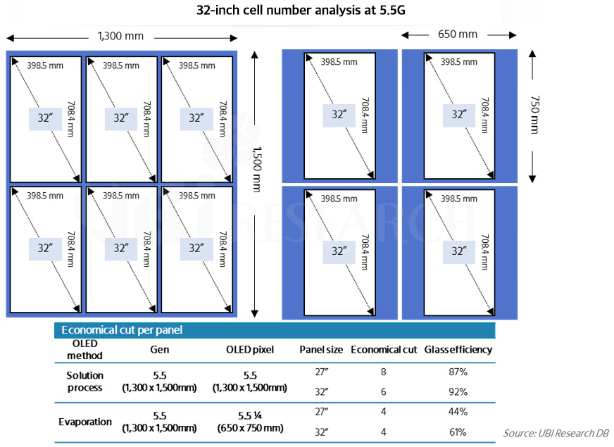
If the 27-inch and 32-inch OLED panels, which are mainly used as gaming monitors, are produced by the FMM method, four can be produced. But sol OLEDs do not divide the substrate, so the 27-inch can make eight, and the 32-inch can make six.
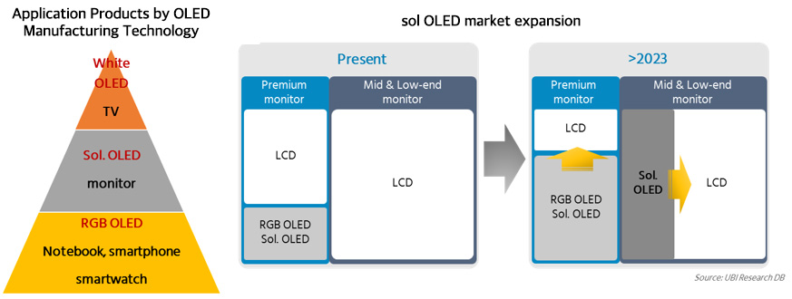
Therefore, in the future, OLED manufacturing technology is expected to be used in combination of three technologies depending on the application and size. Smartphone OLEDs are expected to be divided into FMM and evaporation methods, large OLED panel manufacturing for TVs with open mask and evaporation technology, and sol OLED technology for monitors larger than 25 inches.
There are three types of premium monitor market, LCD, RGB OLED, and sol OLED, but the premium OLED monitor market will be replaced by sol OLED. If 6G-class inkjet lines are invested in large quantities, sol OLED will become the flagship product in the mid-priced monitor market.
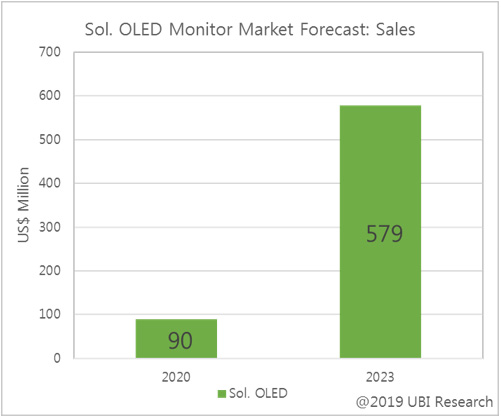
The solution process OLED annual report, published by UBI Research (www.ubiresearch.com), expects to create a market of $ 579 million by 2023. This amount represents 85.3% of the OLED monitor market by 2023.
Contents
| 1. Key Summary
2. Solution Process OLED Overview 3. Necessity of Solution Process 4. Competitive Comparison between Solution Process and Evaporation 5. Solution Process Commercialization Key Issue Analysis 6. Solution Process OLED Monitor Market Entry Scenario |
7. Solution Process OLED TV Market Entry Scenario 7.1 TV size is getting bigger 7.2 Possibility of Solution Process OLED to Enter TV Market 8. Solution Process OLED Technology Issue Analysis 9. Current Status and Development Trend of Solution Process OLED Business of Panel Companies 10. Analysis of Soluble OLED Emitting Material Development Trend 11. Pixel Forming Equipment Supply Chain 12. Solution Process OLED Market Forecast 13. Solution Process OLED Exhibition History 14. Epson Patent Arrangement |
Report Sample
Previous Report Status
Related Products
-
2021 Inkjet Technology Trend for Display Report
₩5,000,000October 22, 2021
This report focuses on inkjet devices and technologies used in OLED and QLED. Inkjet equipment was created by separating the companies that manufacture inkjet heads and systems.
As inkjet head makers, Fujifilm Dimatix, Epson, Konica Minolta, Ricoh, Xaar, and Panasonic were mentioned, and OLED encapsulation equipment makers Kateeva and UniJet were described.
Litrex, TEL (Tokyo Electron), Kateeva, Panasonic Production Engineering, and Toray Engineering are mentioned as inkjet device manufacturers used for Sol OLED. -

Small Sized AMOLED Manufacturing Process Report Ver. 6
₩4,000,000March 8, 2024
The Small Sized AMOLED Manufacturing Process Report covers the manufacturing process for each type of TFT, including LTPS and LTPO TFT, as well as OLED structure and manufacturing process, inspection process, and module manufacturing process.
In this small sized AMOLED manufacturing process report, the Galaxy Z Fold5 structure and module process have been updated for the small OLED manufacturing process. In addition, the eLEAP process and SEL’s photolithography process, which are photolithography OLED processes that have attracted great attention as high-resolution microdisplay OLED manufacturing processes, have been newly added or updated.
This report is a must-read for display companies to understand the AMOLED manufacturing process from TFT substrate to module manufacturing. -
Middle and Large Sized AMOLED Manufacturing Process Report Ver. 6
₩4,000,000March 8, 2024
This report covers the manufacturing process of each type of TFT, including LTPO and Oxide TFT, as well as the structure and cell manufacturing process of OLEDs.
The MLA (micro lens array) formation process for enhancing the brightness of WOLED TVs and the encapsulation process for QD-OLED TVs have been added to the medium and large AMOLED manufacturing process report. Also newly added or updated are the Oxide TFT process with a reduced number of masks, and the eLEAP process and SEL’s photolithography process, which are photolithography OLED processes that have recently attracted great attention as new 8th generation substrate OLED manufacturing processes.
This report will be a must-read for display companies to understand the AMOLED manufacturing process from TFT substrate to cell manufacturing.